
Samsung Targets 2028 for High-NA EUV DRAM Production
Samsung says it plans to use ASML’s higher-resolution High-NA EUV lithography for high-volume DRAM manufacturing by 2028.
What you need to know
- Samsung and ASML expanded their semiconductor manufacturing partnership on 8 September 2026.
- Samsung plans High-NA EUV for high-volume DRAM production by 2028.
- The companies are also backing a shift from 6-inch to 12-inch photomasks.
Samsung Electronics has said it plans to introduce ASML’s High Numerical Aperture EUV lithography into high-volume DRAM manufacturing by 2028, following an expanded semiconductor partnership announced on Tuesday 8 September.
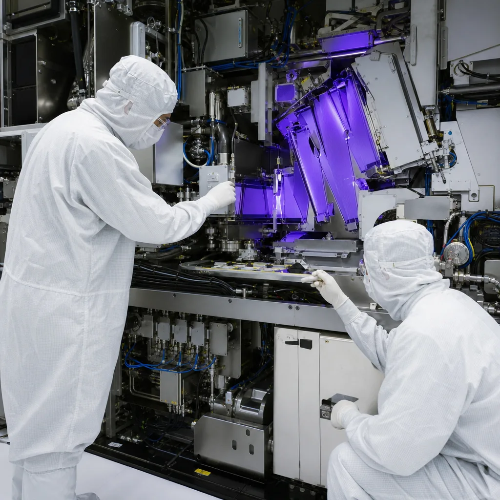
Samsung and ASML describe it as the industry’s first planned use of High-NA EUV in high-volume DRAM production. It remains a forward-looking target rather than confirmation that Samsung has begun production or that the schedule is assured.
Finer patterns for future memory
High-NA EUV is ASML’s newer EXE platform, which raises numerical aperture from 0.33 on existing NXE EUV tools to 0.55. According to ASML, the systems use a 13.5nm EUV light source and offer 8nm resolution, compared with around 13nm for the NXE platform.
That higher resolution allows chipmakers to print finer patterns. ASML says its EXE:5200B system can print single-exposure features 1.7 times smaller than its NXE systems, with potential transistor densities 2.9 times higher under its stated comparison.
Samsung has not confirmed which High-NA machine it will use, where its planned DRAM production will take place, or which memory products may result.
Why masks are part of the plan
The partnership also covers next-generation photomasks. Samsung said it will join an industry initiative to develop a 12-inch photomask platform for High-NA EUV, replacing the 6-inch format traditionally used in semiconductor manufacturing.
The larger masks are intended to improve fabrication productivity, lower chipmaking costs and reduce stitching constraints, where multiple exposures are used to create larger designs. ASML chief technology officer Marco Pieters told Reuters that successful industry adoption could increase system productivity by 40%, though that is a potential industry-wide outcome rather than a promised result for Samsung DRAM.
Separately, ASML and TSMC have set a roadmap for a 12-inch mask pilot line by 2031 and for 12-inch High-NA lithography systems to be ready for advanced-node production by 2033. Those dates apply to the wider mask-format effort, not Samsung’s 2028 DRAM target.
Not the first High-NA production use
Samsung’s plan concerns DRAM specifically. High-NA EUV is already being used elsewhere: ASML said Intel Foundry has processed more than one million wafers with the technology across certification, testing, research and development, and volume production on selected layers for a subset of Intel Core Ultra Series 3 processors, codenamed Panther Lake.
For buyers, the significance is longer-term. More capable lithography may eventually help enable denser memory for future phones, PCs and AI-focused hardware, but Samsung has not announced any retail products using this DRAM, nor any price or availability details for the UK.
Why it matters
High-NA EUV could help manufacturers make finer DRAM patterns, supporting denser memory in future electronics. There is no immediate change for UK buyers: Samsung has not named any consumer products, memory capacities, performance figures or UK availability tied to the plan. The 2028 date is a target, not confirmation that production is under way or guaranteed.
Sources and evidence (16)
- news.samsungsemiconductor.com (other)
- pr.tsmc.com (other)
- asml.com (other)
- ourbrand.asml.com (other)
- marketscreener.com (other)
- investing.com (other)
- asml.com (other)
- news.samsungsemiconductor.com (other)
- asml.com (other)
- marketscreener.com (other)
- en.yna.co.kr (other)
- asml.com (other)
- asml.com (other)
- asml.com (other)
- pr.tsmc.com (other)
- investing.com (other)