
JEDEC’s SPHBM4 Standard Could Ease the AI Memory Bottleneck
The newly published SPHBM4 specification aims to deliver HBM4-class bandwidth without relying on the most constrained silicon-interposer packaging.
What you need to know
- JEDEC published its JESD330-4 SPHBM4 memory standard on 13 July 2026.
- SPHBM4 uses HBM4 DRAM stacks but reduces the processor connection from 2,048 signals to 512.
- It could reduce reliance on scarce advanced packaging, but it does not make HBM memory cheap.
JEDEC has published the final SPHBM4 specification
JEDEC has published a new memory standard intended to tackle one of the least glamorous, but most consequential, constraints in AI hardware: getting vast amounts of high-bandwidth memory connected to a processor without relying so heavily on scarce advanced packaging.
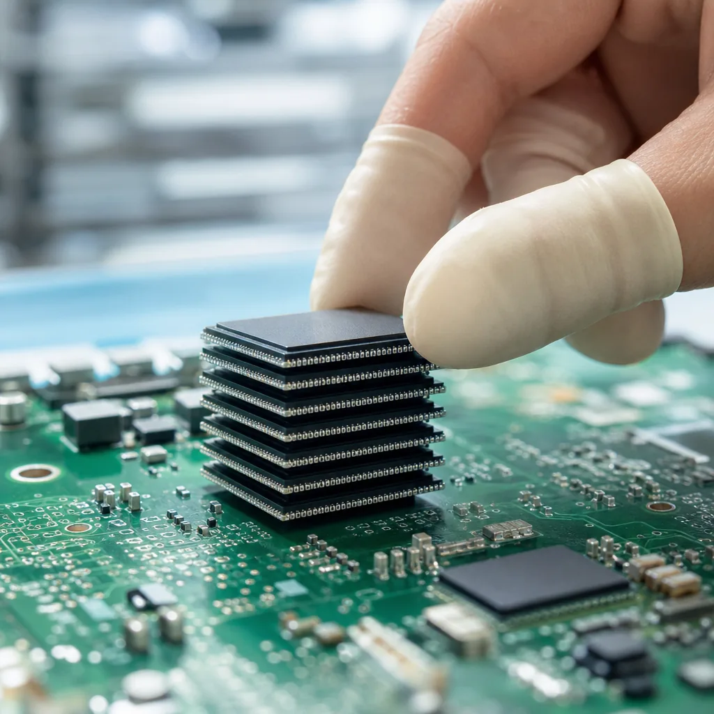
The Solid State Technology Association announced JESD330-4, Standard Package High Bandwidth Memory, or SPHBM4, on 13 July. The completed specification is now available from JEDEC, following an announcement in December 2025 that the organisation was nearing completion of the standard.
SPHBM4 is designed for AI data-centre accelerators, high-performance computing systems and other specialised hardware where memory bandwidth is critical. It is not a replacement for HBM4 memory itself. Instead, it uses the same DRAM stacks as HBM4, with a different interface base die that changes how the memory communicates with the host processor and how it is assembled into a package.
HBM4-class bandwidth with fewer processor connections
Conventional HBM4 uses an exceptionally wide 2,048-signal interface. That helps deliver enormous bandwidth, but it also consumes significant processor silicon area and demands sophisticated package construction. SPHBM4 reduces the interface to 512 signals, using 4:1 serialisation and much higher interface frequencies to make up the difference.
The standard uses 32 independent 16-bit DDR channels, arranged into eight Quad Channels, rather than a 2,048-bit host connection. It supports data rates from 22.4 GT/s to 46.0 GT/s. At its maximum rate, JEDEC specifies peak bandwidth of 2.944 TB/s per memory stack.
That theoretical peak is above the roughly 2 TB/s JEDEC specifies for regular HBM4 operating at 8 GT/s with its 2,048-bit interface. But bandwidth is not the whole performance story. SPHBM4 does not make the underlying DRAM array faster, as the HBM4 memory core retains the same fundamental architecture and timings. The additional physical interface circuitry is also expected to introduce some latency.
For reliability at its high transfer rates, each Quad Channel shares a command and address interface protected by forward error correction. Data transfers use dedicated differential write and read clocks, alongside ECC and error-reporting signals.
The packaging change is the important part
The principal attraction is not simply a bigger headline bandwidth number. SPHBM4 is specified to support bump pitches above 90 micrometres and channel reaches of up to 20mm. Those properties make it possible to mount HBM stacks on standard organic substrates rather than silicon substrates.
That could remove the need for an expensive silicon interposer in this part of an AI accelerator package, while reducing dependence on advanced packaging technologies such as TSMC’s CoWoS. Those packaging methods are a limited resource, even as memory makers expand DRAM production to address AI demand.
The shift could also improve memory density around a processor. With HBM mounted on silicon substrates, stacks must sit immediately beside the XPU, limiting a 25mm die edge to two stacks. JEDEC’s SPHBM4 approach allows three memory devices along the same edge on an organic substrate, increasing potential memory capacity and bandwidth by approximately 50%.
SPHBM4 supports stacks containing four, eight, 12 or 16 DRAM dies, using 24Gb or 32Gb densities. Its largest standardised configuration is therefore a 64GB stack made from sixteen 32Gb dies, matching the maximum capacity supported by HBM4E.
Cheaper packaging does not automatically mean cheap memory
The standard should not be read as a promise of low-cost HBM. SPHBM4 still requires large HBM4 DRAM chips, 2.5D packaging, a complex base die and advanced assembly involving through-silicon vias. The new base die may itself cost more than the base die used by conventional HBM4.
There are further variables before a real-world verdict is possible. Latency, power consumption, signal integrity, controller complexity and workload performance will vary according to the final memory stack, base die, package design and host processor. A high aggregate bandwidth figure does not ensure identical behaviour to a conventional HBM4 implementation.
JEDEC has not announced any products based on the completed standard, nor has it provided deployment dates, UK pricing or named hardware partners. An accompanying SPHBM4 Bump Map addendum, JESD330-4-1, is currently available only to members of JEDEC’s JC-42 committee and will be posted publicly if approved by the organisation’s board.
What it means for UK buyers
SPHBM4 will not appear as a general-purpose memory upgrade or in the next mainstream gaming graphics card. HBM remains considerably more complex and expensive than GDDR7, and its immediate market is data-centre accelerators and high-performance computing.
Its consumer relevance is indirect but potentially meaningful. HBM demand and the specialist packaging needed to deploy it have become a bottleneck for AI hardware. If SPHBM4 lets accelerator builders use less constrained packaging while maintaining HBM4-class throughput, it could eventually ease build-cost pressure for AI infrastructure. That may, over time, feed into the pricing and availability of AI cloud services and the AI features increasingly offered through PCs and phones. For now, however, the standard is a foundation for future products rather than a confirmed price cut.
Why it matters
SPHBM4 is not memory for the next gaming PC or graphics card, but it could matter indirectly to UK buyers. If it helps AI accelerator makers avoid constrained advanced packaging capacity, it may eventually reduce cost pressure on the cloud infrastructure behind AI services and AI features in consumer devices. That outcome is not guaranteed: final costs and performance will depend on the memory, package and processor designs that adopt the standard.